Final Robot
Printed Circuit Board
As encouraged by the course staff, we decided to make a printed circuit board (PCB) to both clean up our wiring for our final robot and to remove the problem of wires falling out that is inherent when using a breadboard. The idea for the PCB is that the PCB would sit like a ‘hat’ on the Arduino and have headers for all sensors and other inputs. We used EAGLE PCB Design Software to design the PCB.
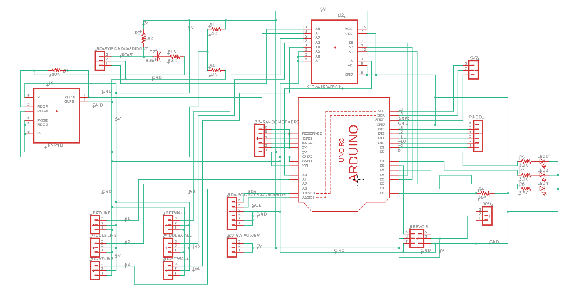
The first step in this process was creating the schematic. This involved downloading all the parts we are using from online libraries and wiring everything as we have on the breadboards. I downloaded a library for the multiplexor and for the Arduino to ensure the dimensions of the pinouts and spaces were all correct. Here is a picture of the schematic.
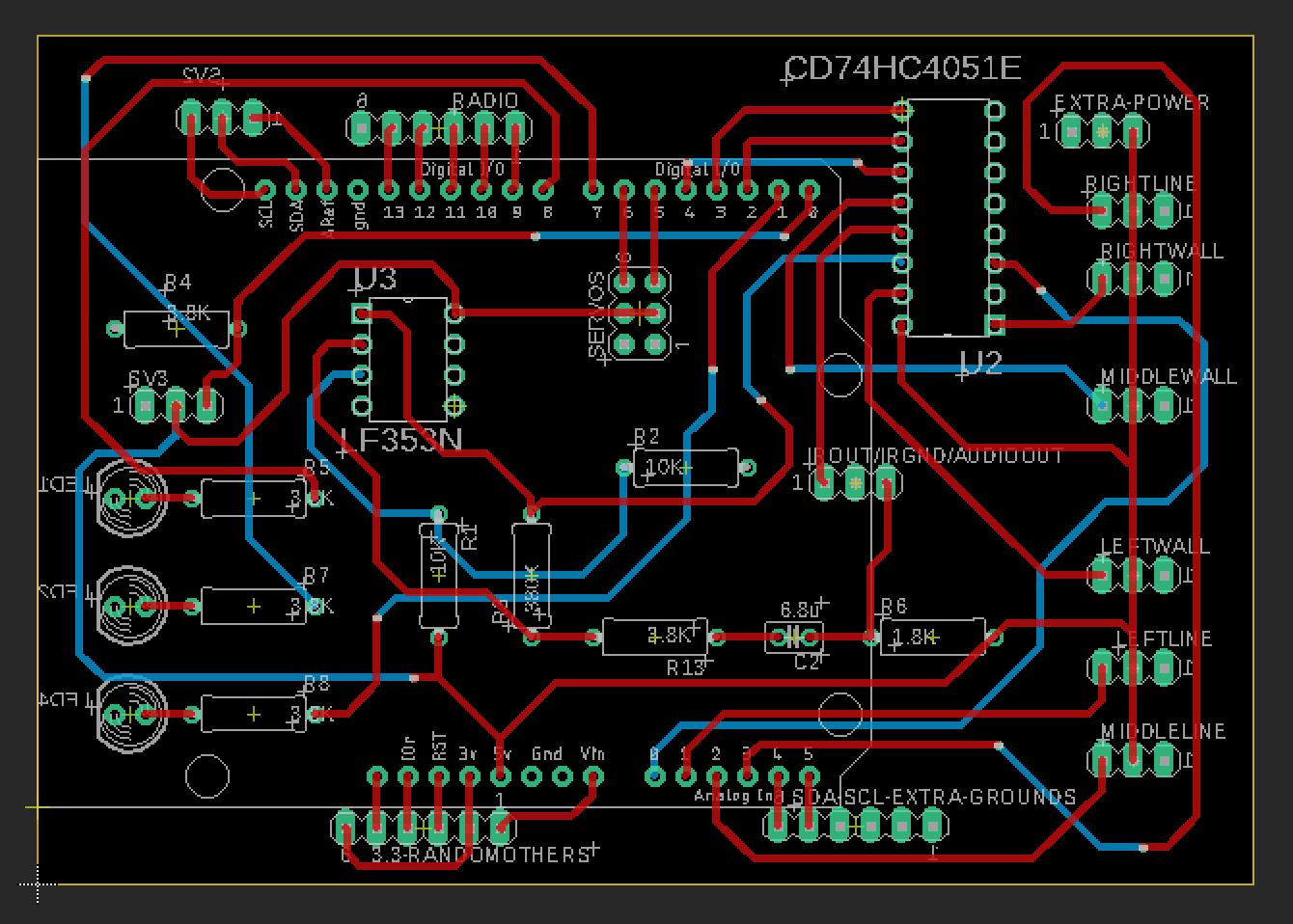
The next part of the process was to use the schematic to layout the board. First I placed all components on the board. When placing the components on the board, all pins on each omponent have straight ‘air wires’ that show which pins on other components the given pin needs to be wired to. So, when placing the components, it is most ideal to have as few ‘air wires’ crossing eachother as to make wiring the components easier later.
We chose to have a 2-layer board. The bottom layer is ground. This simplifies the wiring because it allows all pins that need to be grounded to be shorted to the bottom layer instead of all being wired together. After creating the ground layer, we started connecting the wiring on the top layer. After choosing a trace width of about 0.6 mm as determined by the max voltage of 5V, with as straight wires as posible, we wired all components together. Because some wires cross, some wires need to go through a via to the bottom layer to go under the wires they intersect with when being routed. Here is a picture of the schematic. Red wires are throuhg the top layer and blue wires are through the bottom layer.
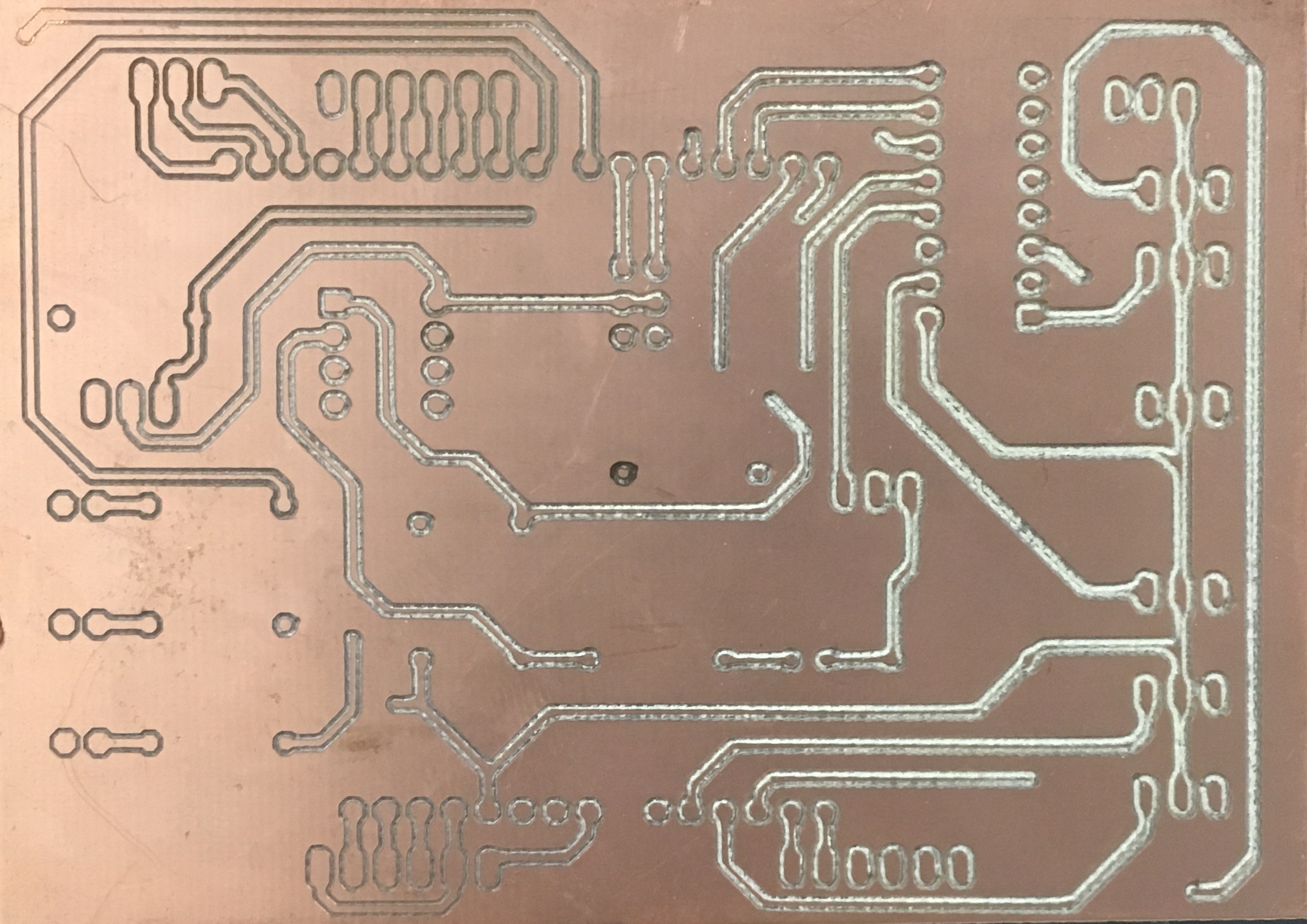
The PCB ultimately failed because of the PCB mill we used to print it. We were not able to level the board properly so each time we milled the board, some parts of the board were cut to deep so there was no path for signal, and in some place its was not cut deep enough and the copper was not broken through and thus the signal was shorted with the whole level. We tried for a long time to level the board but we eventually gave up. We realized that even if we finally printed the first side correctly by luck, we would also have to print the second side perfectly. Since we would not be so lucky twice in a row, we decided to give up on the PCB and put our circuitry on protoboards.
Below is a picture of a failed protoboard. On the top left of the board, you can see that the mill did not cut through the copper so that trace would be shorted with the rest of the layer. At the same time, on the right side, the mill cut so deep that there is no copper left to transport the signal. This issue was caused by the uneven base of the mill. This caused us to put our circuit on a protoboard instead of using the PCB.
Proto Boarding
Once we realized that the printed circuit board would not work, we decided to move all our circuitry to protoboards. We moved the amplifiers, multiplexer, headers, LEDs, and microphone to small protoboards cut to the needed size as to be as small as possible. We used protoboards that had rows of holes connected by small copper pieces that immitate a breadboard to clean up the soldering work.